Current
location:
Current
location: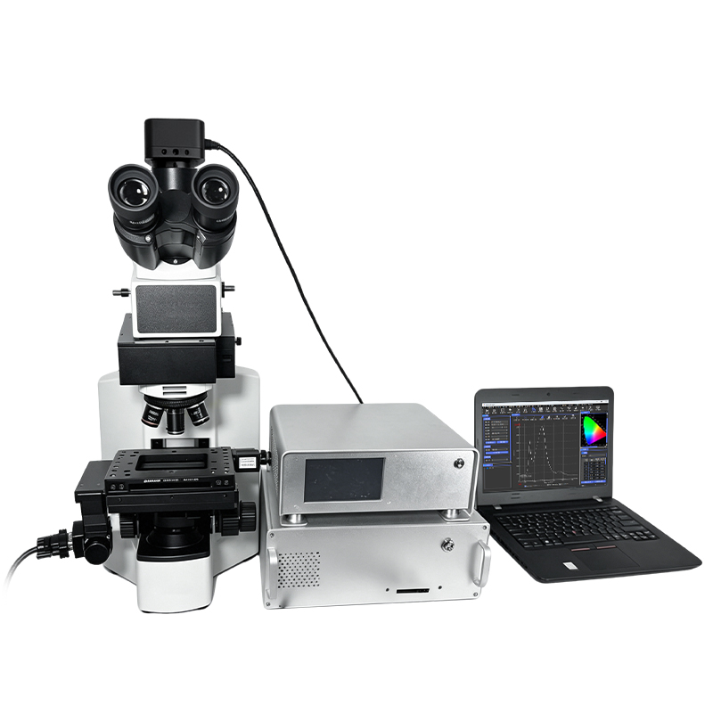


Product Introduction
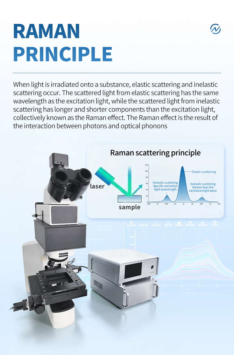
In semiconductor fabrication and advanced materials research, understanding the spatial distribution of chemical phases, stress states, and compositional variations across a sample surface is not optional — it is fundamental to process control and discovery. Single-point Raman measurements, while spectroscopically rich, provide only isolated snapshots that may miss critical heterogeneity. Confocal microscopes offer spatial resolution but lack molecular specificity. And synchrotron-based techniques, while powerful, require beamtime access that most laboratories simply cannot secure for routine work.
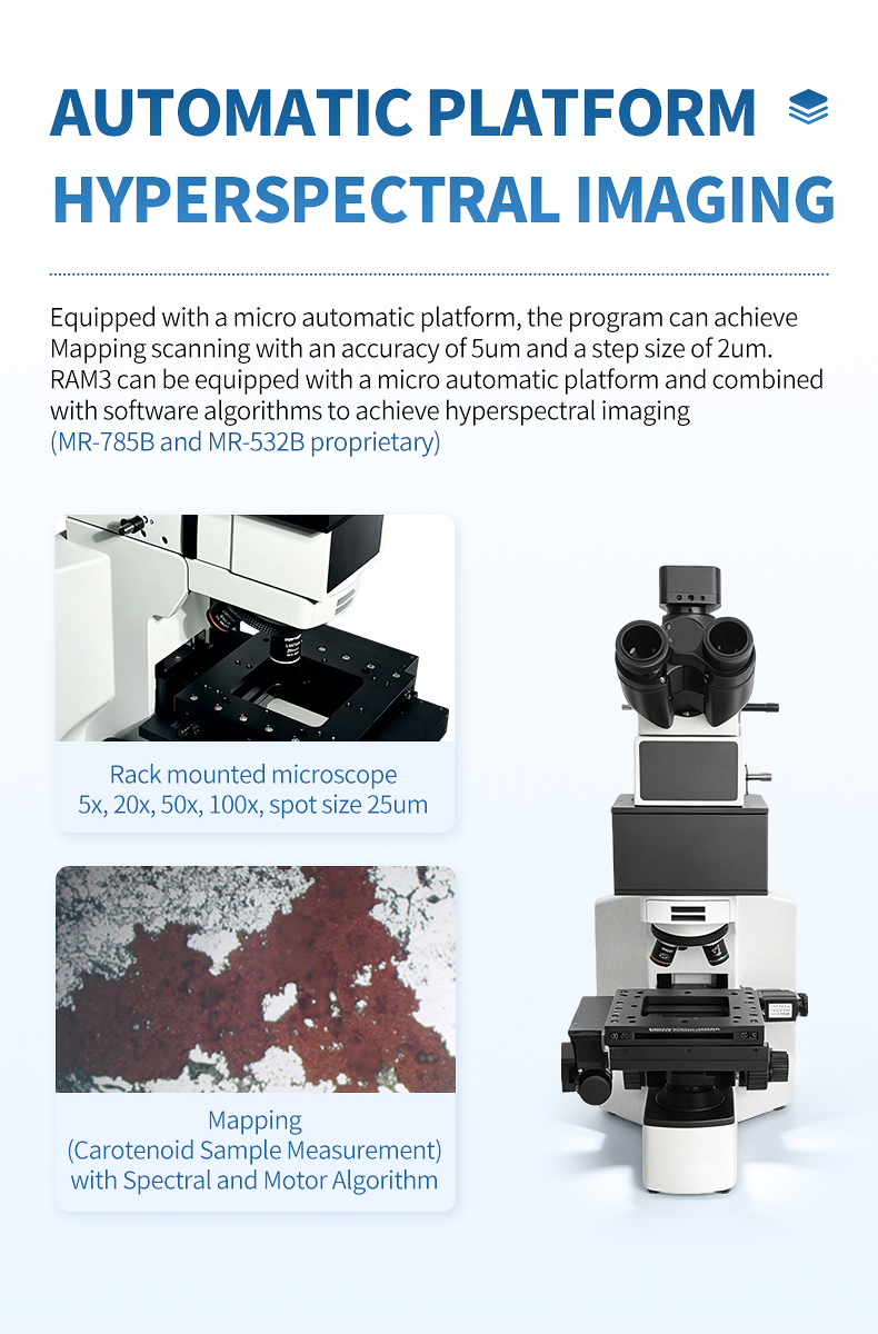
The MR-532B micro Raman mapping spectrometer bridges this gap by combining the molecular specificity of Raman spectroscopy with automated two-dimensional spatial scanning. Its motorized X-Y stage traverses a 110 mm × 75 mm range with 5 μm positioning accuracy and 2 μm minimum step size, systematically collecting a full Raman spectrum at every grid point. Integrated autofocus tracking continuously compensates for sample surface topography — essential when mapping cleaved semiconductor wafers, polished mineral sections, or tablet cross-sections where surface height varies by tens of micrometers.
The 532 nm excitation wavelength provides inherently strong Raman scattering from silicon (the 520.7 cm⁻¹ phonon peak shifts measurably under strain), carbon allotropes (D, G, and 2D bands reveal structural order), and crystalline minerals (lattice modes identify phase transitions). With the Hamamatsu 11639 CMOS detector delivering 2048 pixels and 7 cm⁻¹ spectral resolution, the MR-532B captures the subtle peak shifts, intensity ratios, and bandwidth changes that encode chemical and structural information at every pixel.
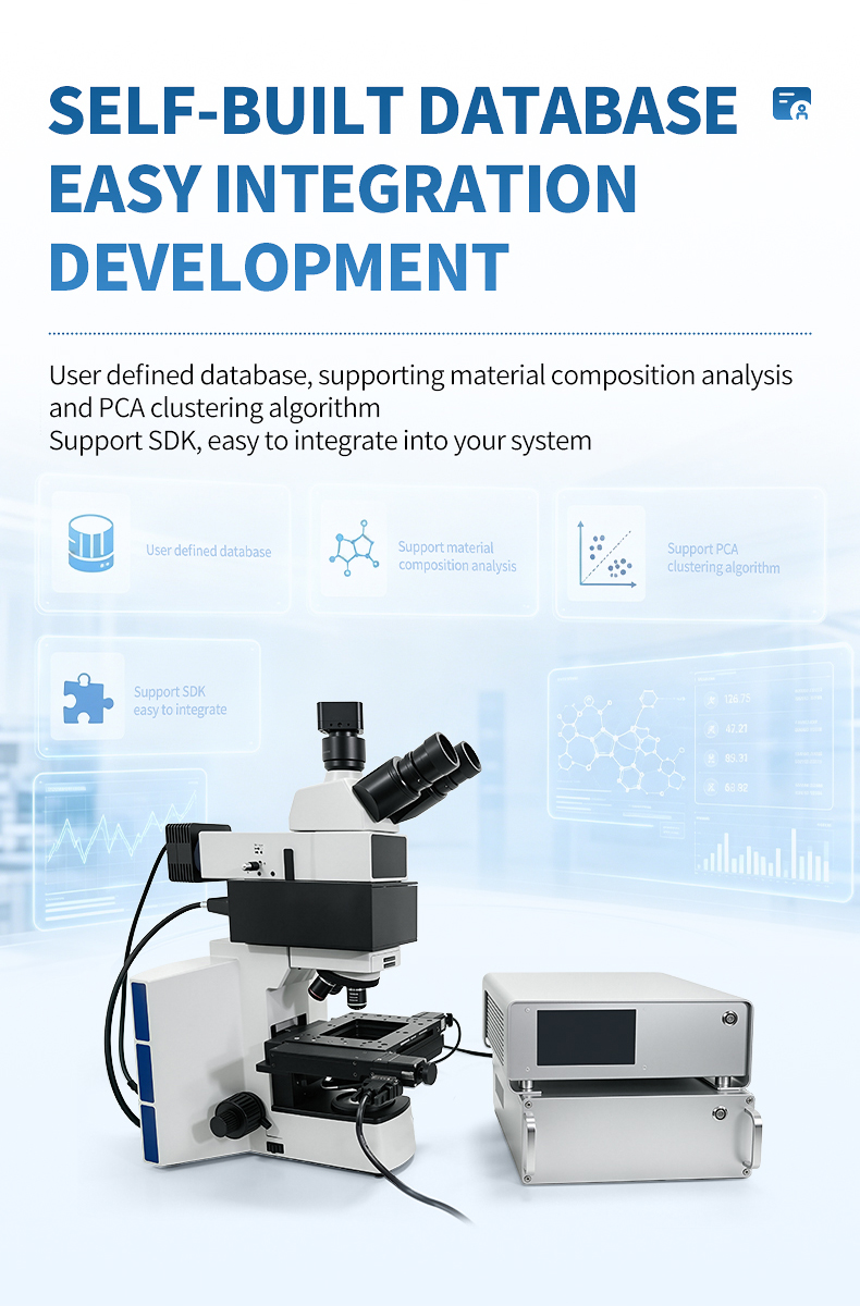
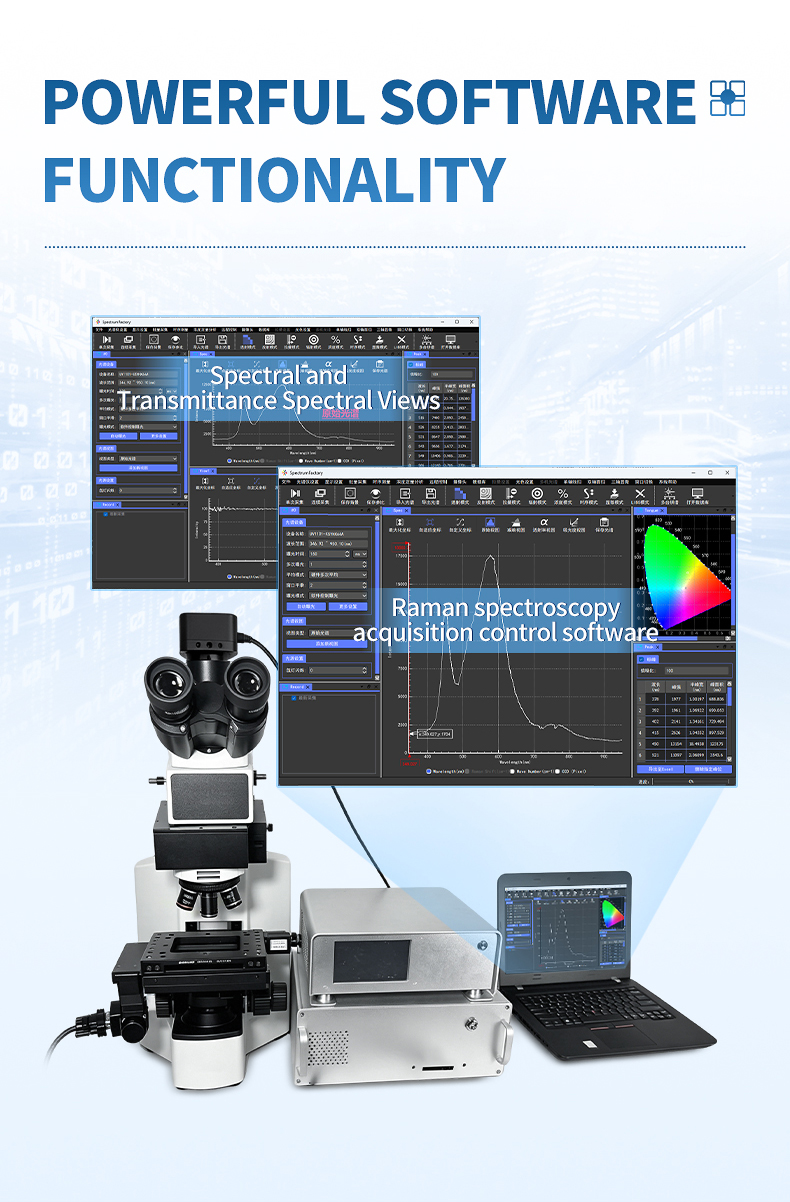
SpectrumFactory software orchestrates the entire mapping workflow: users define regions of interest on the live microscope image, set grid spacing and integration parameters, and launch unattended acquisitions. Post-processing applies baseline correction, performs PCA clustering to identify chemically distinct domains, and generates publication-ready false-color chemical maps. For researchers investigating semiconductor strain engineering, carbon film uniformity, or mineral paragenesis, the MR-532B transforms point spectroscopy into comprehensive spatial analytics. See our Raman applications in materials science for detailed case studies.
Applications
- Semiconductor wafer stress mapping — Quantify biaxial stress distribution across Si, SiGe, and GaN wafers by tracking the 520.7 cm⁻¹ phonon peak shift with sub-wavenumber precision at every grid point
- Carbon film uniformity assessment — Map D/G band intensity ratios and 2D band profiles across CVD graphene, DLC coatings, and carbon nanotube arrays to evaluate synthesis quality over large areas
- Mineral phase distribution in thin sections — Generate spatial maps of mineral assemblages in petrographic thin sections for paragenetic sequence analysis and ore deposit characterization
- Pharmaceutical API distribution in tablets — Visualize active ingredient homogeneity and excipient segregation in tablet cross-sections for formulation development and process validation
- Microplastic particle identification on filters — Automated scanning of filter membranes to identify, classify, and spatially map microplastic particles by polymer type with spectral library matching
- Coating and thin film compositional analysis — Map layer composition, thickness uniformity, and interdiffusion zones in multilayer coatings and functional thin films
- Art conservation pigment mapping — Non-destructive identification and spatial distribution of historical pigments, binders, and degradation products across painted surfaces
- Forensic trace evidence area scanning — Systematic search and identification of fibers, paint chips, explosive residues, and drug particles on evidence collection substrates
Key Features and Advantages
- Motorized X-Y stage with 5 μm positioning accuracy and 2 μm step size enables chemical imaging at spatial resolutions approaching single-cell and single-grain scales
- 110 mm × 75 mm travel range accommodates full semiconductor wafers, large geological thin sections, and pharmaceutical tablet arrays without manual repositioning
- Integrated autofocus tracking dynamically adjusts focal position during scanning, maintaining optimal signal quality across samples with surface height variations up to several millimeters
- 532 nm excitation provides 3.5x stronger Raman scattering than 785 nm, enabling shorter dwell times per pixel and faster total mapping time for high-throughput workflows
- 1800 gl/mm grating blazed at 500 nm delivers 7 cm⁻¹ resolution, sufficient to detect stress-induced silicon phonon shifts of less than 1 cm⁻¹ for quantitative strain analysis
- Hamamatsu CMOS detector with 2048 pixels and >99.8% linearity supports quantitative peak ratio analysis essential for carbon material characterization (D/G, G/2D band ratios)
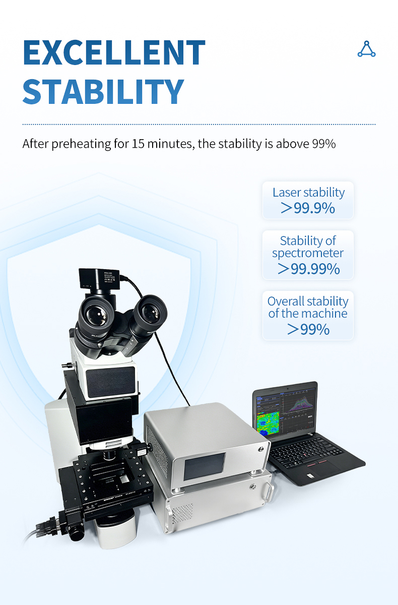
- System stability >99% over 8 hours enables overnight unattended mapping of large grids (e.g., 100 × 100 pixels) with consistent spectral quality from first to last point
- SpectrumFactory mapping module automates the complete pipeline: ROI definition, grid generation, spectral acquisition, preprocessing (airPLS baseline, smoothing), and chemical image export
- PCA clustering analysis identifies chemically distinct regions within mapping datasets without prior knowledge, revealing hidden heterogeneity and unexpected phase distributions
- SMA905 fiber optic interface and GPIO outputs support synchronization with external stages, environmental chambers, or automated sample handling systems for custom configurations
- External trigger input with 5 ns latency enables precise hardware synchronization for time-resolved or position-correlated measurements in automated production-line inspection
- Four objective magnifications (5x–100x) allow users to select optimal trade-off between spatial resolution and mapping area, from survey scans to single-particle analysis
- Data export in standard formats (CSV, SPC, image files) integrates with third-party analysis platforms including MATLAB, Python, and commercial spectroscopy software
- Compact rack-mounted design with standard AC power requirement enables installation in any laboratory without dedicated infrastructure modifications
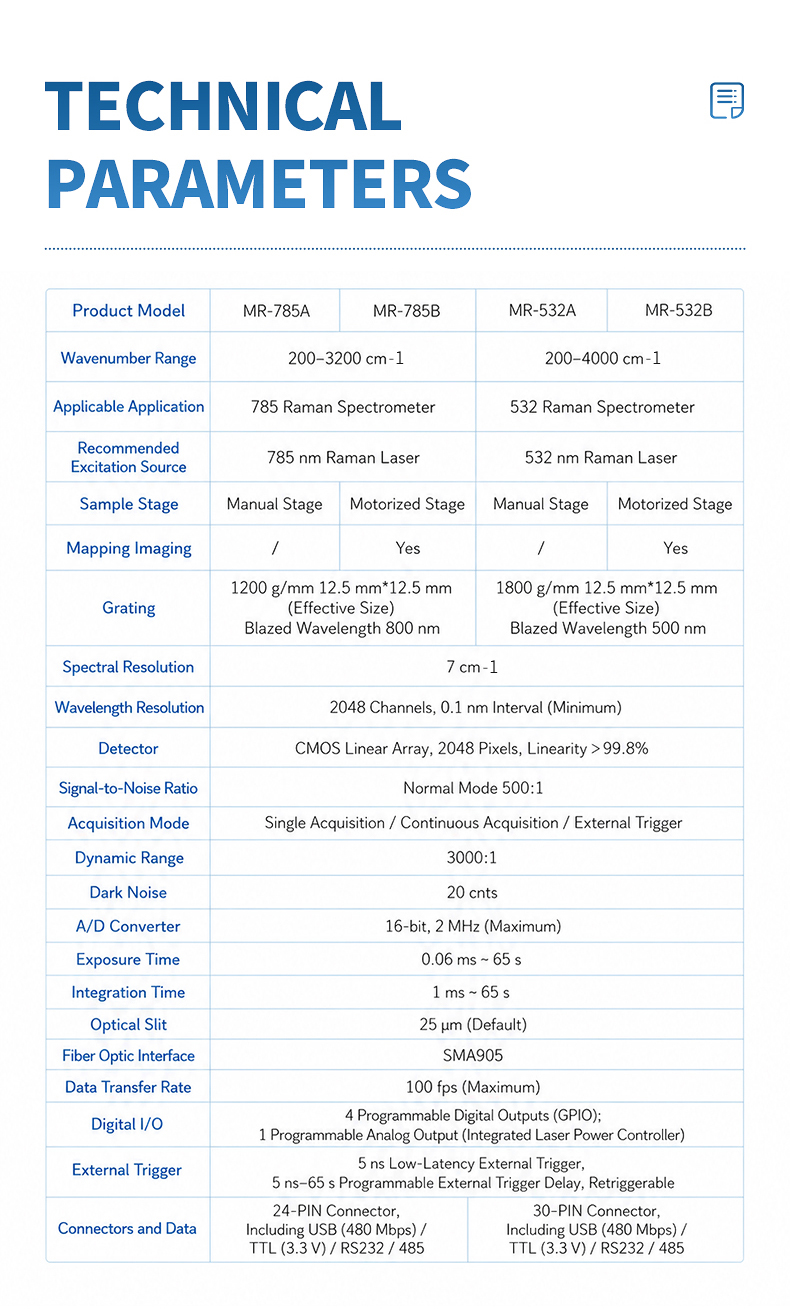
Technical Specifications
| Parameter | Specification |
|---|---|
| Product Model | MR-532B |
| Excitation Wavelength | 532 nm |
| Wavenumber Range | 200–4000 cm⁻¹ |
| Spectral Resolution | 7 cm⁻¹ |
| Grating | 1800 gl/mm, 12.5 mm × 12.5 mm, blazed at 500 nm |
| Detector | Hamamatsu CMOS linear array, 2048 pixels, linearity > 99.8% |
| Wavelength Resolution | 2048 channels, 0.1 nm interval (minimum) |
| Signal-to-Noise Ratio | 500:1 (normal mode) |
| Dynamic Range | 3000:1 |
| Dark Noise | 20 counts |
| A/D Converter | 16-bit, 2 MHz (maximum) |
| Acquisition Mode | Single / Continuous / External trigger / Mapping grid |
| Exposure Time | 0.06 ms – 65 s |
| Integration Time | 1 ms – 65 s |
| Optical Slit | 25 μm (default) |
| Sample Stage | Motorized mapping platform |
| Stage Travel Range | X: 110 mm, Y: 75 mm |
| Positioning Accuracy | 5 μm |
| Minimum Step Size | 2 μm |
| Autofocus | Integrated focus tracking for mapping |
| Microscope | Rack-mounted, 5x / 20x / 50x / 100x objectives |
| Spot Size | 25 μm |
| Fiber Optic Interface | SMA905 |
| Data Transfer Rate | 100 fps (maximum) |
| Digital I/O | 4 programmable GPIO; 1 analog output |
| External Trigger | 5 ns latency, 5 ns–65 s delay, retriggerable |
| Connectors | 30-pin (USB 480 Mbps / TTL 3.3 V / RS232 / RS485) |
| System Stability | Laser >99.9%, Spectrometer >99.99%, Overall >99% (8h after 15-min warm-up) |
FAQ
Q: What spatial resolution can I achieve with Raman mapping on the MR-532B?
A: With the 100x objective, the 532 nm spot is approximately 25 μm. The stage supports 2 μm step sizes for oversampled mapping. The 5x objective enables survey mapping of large areas, while 20x and 50x offer intermediate resolution.
Q: How long does a typical Raman mapping experiment take?
A: A 50 × 50 grid with 1-second integration takes approximately 45–60 minutes. A 100 × 100 grid requires 3–4 hours. The 8-hour stability ensures consistent data quality for overnight mappings without drift correction.
Q: Can the MR-532B detect stress in silicon wafers quantitatively?
A: Yes. The silicon phonon peak at 520.7 cm⁻¹ shifts linearly with stress at approximately −2.0 cm⁻¹/GPa. With 7 cm⁻¹ resolution and curve fitting, peak positions can be determined with sub-wavenumber precision, enabling stress quantification better than 50 MPa sensitivity.
Q: How does autofocus tracking work during mapping?
A: The autofocus continuously monitors surface position and adjusts Z-axis to maintain optimal focus. This is essential for samples with topography variations of even 10–20 μm, adding minimal overhead to total mapping time.
Q: What output formats does the mapping software support?
A: SpectrumFactory exports spectra as CSV or SPC, chemical maps as PNG/TIFF/BMP, and complete datasets as project files. PCA results can be exported as component maps. Raw data imports into MATLAB, Python, R, or commercial platforms for custom analysis.
Q: Can the system handle irregularly shaped or fragile samples?
A: Yes. Manual stage adapters accommodate non-standard geometries including irregular fragments and curved surfaces. The autofocus compensates for surface irregularities, and the 25 μm working distance of the 50x objective provides adequate clearance.
Article address:https://www.spectrometer.top/micro-raman-spectrometer/raman-mapping-semiconductor-materials-research.html